
Blameless 150 схема
Обновлено: 07.07.2024
Update:
Implementing DC-offset correction Post Nr 16
Update History
2019-03-20: Implementing DC-offset correction Post Nr 16
2019-03-18: Implementing the Vbe multiplier and the current limiting. Post Nr 15
2019-03-16: after a while and other projects, I am back to this one and changed the topology: Post Nr 11
Orginal Post / Start:
Here is my first design of upcoming project. A lot is based upon Douglas Self Book and other, earlier Amps which I made. But I am really interessted in your Ideas.
The amp is called NoHyprid . and guess a Hyprid version will follow. But first I want to build up conventional with Transistors before I throw in some tubes. Thats why i use NPN BJT in the input stage.
The input is a cascode working on a current mirror. Followed by a EF-VAS (that was rather new to me - thanks Douglas Self).
The output is build up conventionally by 2-stage emitter followers. Power BJT are not chosen jet.
Well, some times passed by. This one never got out of the simulation, so I started again and need to finish till summer. The goal is to have a board which supports BJT or tubes as input devices.
Any thoughts? Simulation works pretty well, but was not easy to get the OPs stable. Real world test will be exciting
Vbe multiplier and protection parts are missing at the moment.
Attached Images| Blameless-BJT.jpg (87.4 KB, 341 views) | |
| Blameless-Hyprid.jpg (86.6 KB, 350 views) |
Not quite sure if the sims are realistic, but THD seems to be very nice:
for the tube/BJT hyprid:
Total Harmonic Distortion: 0.000714% (0.00057% 2nd; 0,00006% 3rd, and 0.0001% 4th) @200W and 4ohms
for the BJT version:
Total Harmonic Distortion: 0.000926% @200W and 4ohms; manly 3rd order
funny, that the tube version has lower harmonics. I guess these results are way to good to be realistic, but it seems that the circut will work.
Will do some versions with Mosfets.
If you are hoping to build a "bootstrapped cascode" for the input stage, so that VCE of the input transistors Q0a and Q0b remains fixed and constant even when the input signal is a 1 kHz sinewave swinging � 1.5 volts .
then the 1uF capacitor "C2" is hurting, not helping. You want the emitters of the cascode transistors Q2a, Q2b to exactly follow the emitters of the differential pair. C2 hurts this.
Thanks, for your comment! Actually I am aware of it, and I tried different things with the tube input. It seems, that a triode with low anode resistance, works better this way. Not sure about it. For the BJT input you are of course absolutely right and I will change that. Thanks!today's task: implementing the Vbe multiplier and the current limiting. I also changed the pre-pre-driver to MJE340/350 to be on the safe side.
The triple output is a bit tricky to get stable; also with the current limiting circuit. Would be pleased of every input to get it even further stable. Now in simulation it works great, but I am afraid, the real world looks different.
Actually its my first triple output stage.
Also changed the VA-feedback into output inclusive circuit. Seems to be way more stable. Simulations with the tube input stage will follow. Also OPs with Mos-Fets and Quasi-complimentary.
Attached Images| Blameless-BJT-Climit.jpg (100.3 KB, 183 views) |
Adding Offset correction.
Still would be pleased for any kind of input. Still worried about stabilisation, even if the simulations looks fine.

Versi final.

Ini adalah prototype KIT Blameless 150. Artikel bisa dibaca di sini.
PCB sudah tersedia. Bahan PCB ada yang dari fiber dan ada yang pertinak.

PCB pertinak:

PCB fiber:

Jalur tembaga:
Ukuran PCB 163 mm x 116 mm.
Kualitas suara secara subyektif tidak kalah dengan VSSA.
CARA PERAKITAN BLAMELESS 150
Urutan pemasangan komponen:
1. Pasang semua jumper dan solder.
2. Pasang semua resistor 0,25W dan solder.
3. Pasang semua dioda, kecuali D3 dan solder.
4. Pasang semua resistor 0,5W dan solder.
5. Pasang semua resistor 1W dan solder.
6. Pasang semua resistor 2W dan solder.
7. Pasang semua resistor 5W dan solder.
8. Pendingin Q10 dan Q11 diberi grease pada permukaan yang akan ditempel Q10 dan Q11.
9. Pasang transistor Q1 sampai Q13 dan solder.
10. Beri lem (misalnya lem UHU) pada pendingin Q10 dan Q11 yang menempel ke PCB.
11. Pasang semua kapasitor, kecuali C7 dan solder.
12. Pasang L1, connector (SL1 dan X1 dipasang salah satu), dan fuse holder. Solder.
13. Pasang Q14 sampai Q20. Q16 sampai Q20 harus dilapisi lembaran mika. Pada permukaan pendingin dan bagian belakang transistor diberi grease. Pastikan semua kaki transistor tidak ada yang terhubung singkat dengan pendingin. Lalu solder.
14. Pasang R25 dan solder.
15. Bodi Q1 dan Q6 diberi grease dan ditempel lalu diikat.
Setting arus bias transistor final dengan multimeter digital:
1. Atur R25 agar nilainya maksimum, sekitar 500 Ohm.
2. Pasang fuse F5A pada fuse holder.
3. Untuk keamanan, seri catu daya positif dan negatif masing-masing dengan lampu pijar 100W.
4. Hidupkan power supply.
5. Ukur tegangan pada J5. Nilai yang wajar dari -200mV sampai +200mV.
6. Ukur tegangan pada R38. Atur R25 agar tegangan pada R38 sebesar 23mV. Diamkan selama 20 menit.
7. Tegangan pada R38 akan sedikit berubah. Atur kembali R25 agar tegangannya sebesar 23mV.
8. Ukur tegangan R38, R39, R42, dan R43. Nilainya maksimal 27mV. Jika ada yang melebihi 27mV, atur ulang R25 agar tegangannya menjadi 27mV.
Jika tidak memiliki multimeter yang bisa mengukur tegangan sekecil 23mV, maka cara setting arus bias adalah sebagai berikut:
1. Atur R25 agar nilainya maksimum, sekitar 500 Ohm.
2. Pasang fuse F5A pada fuse holder.
3. Seri catu daya positif dengan resistor 10 Ohm 2W.
4. Untuk keamanan, seri catu daya positif dan negatif masing-masing dengan lampu pijar 100W.
5. Hidupkan power supply.
6. Ukur tegangan pada J5. Nilai yang wajar dari -200mV sampai +200mV.
7. Ukur tegangan pada resistor 10 Ohm 2W tersebut. Atur R25 agar tegangan pada resistor tersebut antara 1,7V sampai 1,9V.
8. Diamkan selama 20 menit.
9. Jika tegangan pada resistor tersebut berubah, atur kembali.
Jika arus bias sudah selesai diatur, hubungkan catu daya positif dan negatif tanpa diseri dengan apapun. Hubungkan keluaran amplifier ke speaker protector. Amplifier siap digunakan.
Meningkatkan Performa Dengan Matching Komponen
1. Q1 dan Q6 di matching hFE dan VBE.
2. Q2 dan Q5 di matching VBE nya.
3. Q16 dan Q18 di matching hFE nya.
4. Q17 dan Q19 di matching hFE nya.
Matching transistor sebesar 5% sudah cukup baik.
5. R36, R37, R40, R41 di matching sebesar 1%.
6. R38, R39, RR42, dan R43 di matching sebesar 1%.
7. R5 dan R11 di matching sebesar 0,1%.
8. R6 dan R12 di matching sebesar 0,1%.

В качестве усилителя для СЧ и ВЧ динамиков выбрал схему нашего соотечественника Дорофеева. Только схему переделал на современные компоненты, получилось очень дешево, просто и со вкусом, но об этом чуть позже)
Усилитель B класса отличается отсутствием тока покоя выходного каскада ( ну почти).
Из википедии: "Предельный КПД идеального каскада в режиме B на синусоидальном сигнале равен 78,5 %[15], реального транзисторного каскада — примерно 72 %. Эти показатели достигаются только тогда, когда выходная мощность P равна максимально возможной мощности для данного сопротивления нагрузки Pмакс(Rн). С уменьшением выходной мощности КПД падает, а абсолютные потери энергии в усилителе возрастают. При выходной мощности, равной 1/3 Pмакс(Rн), потери реального транзисторного каскада достигают абсолютного максимума в 46 % от Pмакс(Rн), а КПД каскада уменьшается до 40 %. С дальнейшим уменьшением выходной мощности абсолютные потери энергии уменьшаются, но КПД продолжает снижаться" Смысл прост — чем больше наваливаешь, тем меньше греется ( тоже почти).
Вот набросал схему, все просто:
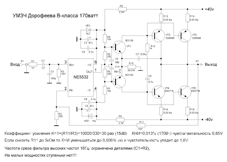
В мультисиме он показывает очень достойные характеристики

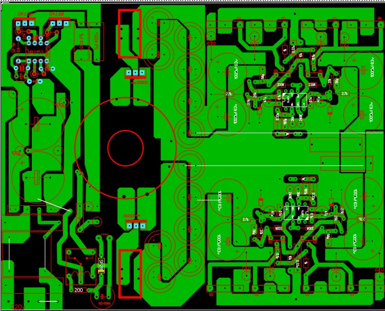
Тут же развел печатку на скорую руку с питанием от сети 220в

Конечно выявил много косяков, но уже позже, цоколевка транзисторов не совпадала, да и ОУ пришлось заменить на менее прожорливую NE5532
Topologi Rangkaian

Читайте также: